project summary
- 2 Wireless Transceivers
- PCB Layout
- Project Lead
skills
- Circuit Design
- PCB Design
- Project Leadership
Background

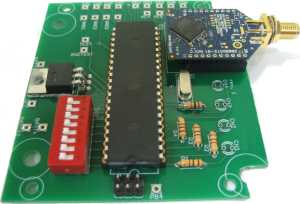
My team was asked to build a special purpose wireless transceiver pair for work with heavy equipment testing. I will not get into the details of the project or the design, but I will say that we were responsible for the parts selection, circuit design, software design, PCB (printed circuit board) design, and the prototype testing and troubleshooting.
Interestingly, there were 2 transceiver boards that were identical but had to fit in different enclosures (hence the two sets of screw holes), had different software, and one of them wired directly to solid state relays whereas the other wired into pushbutton switches and LED indicators.
The interesting functionality of the product (that I CAN disclose) included:
- 2 way communication
- hardware configurable address with software configurable subaddress
- acknowledge of communication and every action with visual feedback
- test mode
- upon request, give visual indication regarding success or failure of communication between transceivers
- upon startup, flash all visual indicators to verify power and that the indicators are not faulty
- long range (I believe it was nearly a mile)
My Role
As the chosen project leader, I interfaced with the customer to identify the project scope including the requirements and additional luxury features. I then led the team by determining which features and functionality the final product would include. I selected the main platform (Atmel AVR microcontroller) and helped the team overcome obstacles in the hardware and software design when necessary. Finally, I designed the PCB’s completely, and they were flawless in their function as well as their physical fit in the chosen enclosures on the first run!
Final Results
The customer loved the product. In fact other groups from the same company in other states ordered some to replace existing inferior solutions!

